Microelectronics and Semiconductor Fabrication Research Internship
PROJECT OVERVIEW
Microelectronics & Nanofabrication Research Internship
During this hands-on internship, I gained cleanroom training and conducted advanced microfabrication experiments on flexible brain electrodes. I applied techniques like photolithography, metal deposition, liftoff, and then analyzed results using profilometry to refine titanium film thickness. I also designed custom patterns using AutoCAD for maskless photolithography, creatively etching visual motifs around a QR code, and learned a valuable lesson in diligence from a gold deposition mishap. I wrapped up my experience by creating an educational video to share fabrication basics with high schoolers.
Introduction to Microelectronics and Nanofabrication
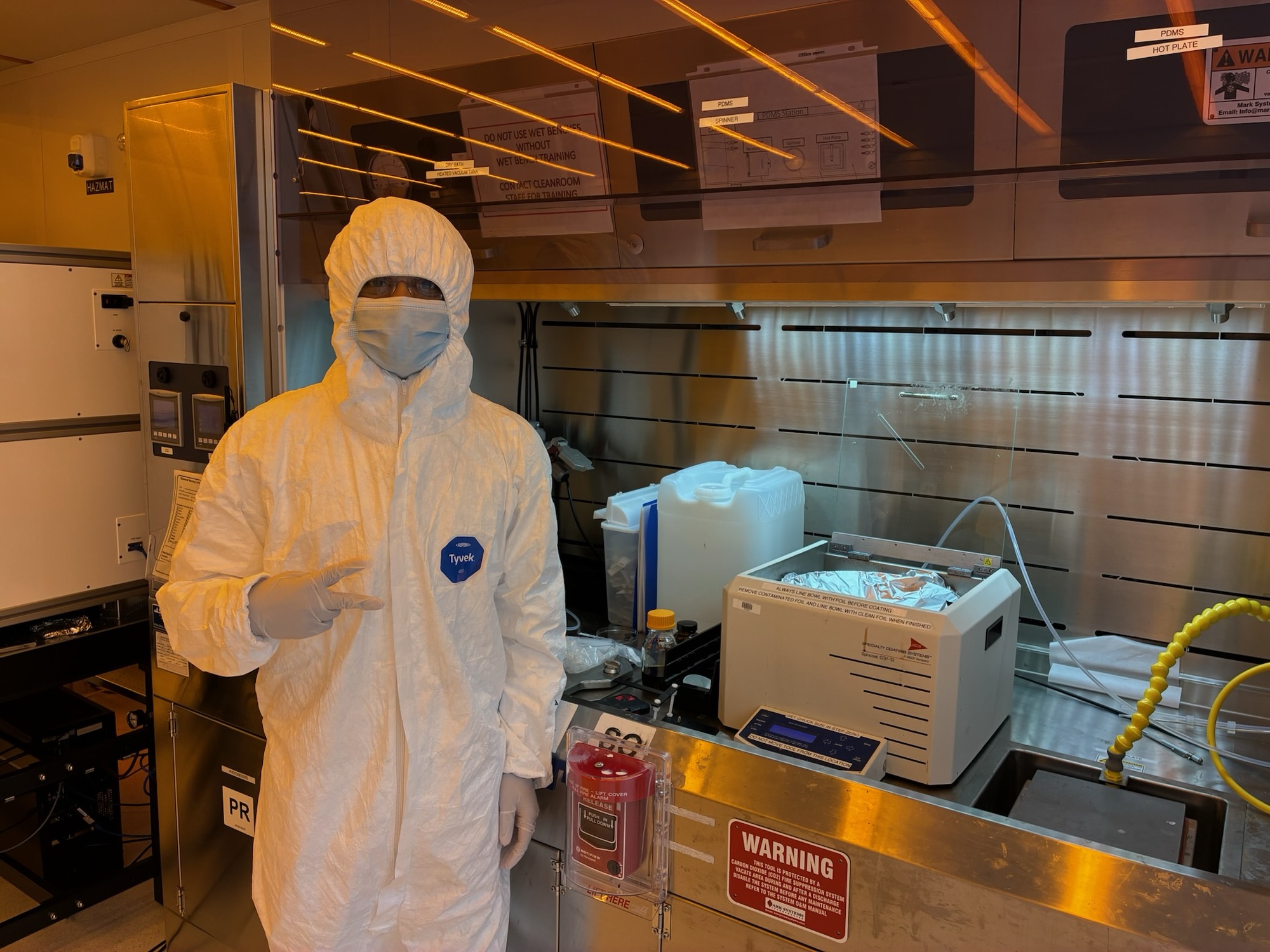
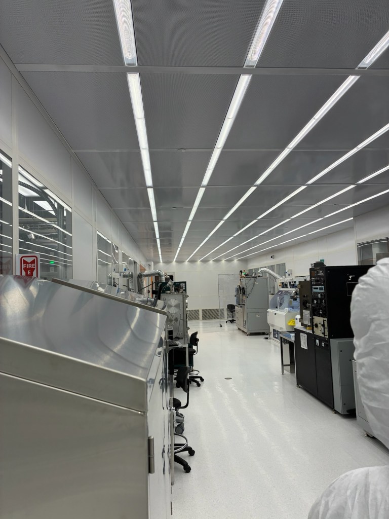
I started my REM: EMProject research internship on microelectronics and nanofabrication by touring the Rice Nanofabrication Facility cleanroom. The internship began with an introduction to the advanced tools and protocols used in nanoscale device fabrication and set the stage for the hands-on research I conducted later in the summer.


Building Foundation

Dr. Yu Kee Ooi led an intensive bootcamp where we reviewed:
- Digital logic design and Semiconductor physics (great refresher from my Rice courses)
- The complete nanofabrication process for semiconductor devices
The highlight was understanding how key cleanroom techniques like photolithography, etching, and metal deposition all work together to create functional devices.
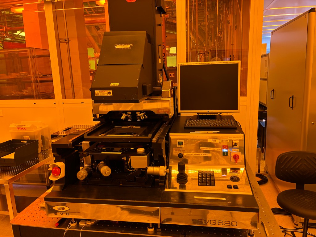
Hands-On in the Cleanroom!
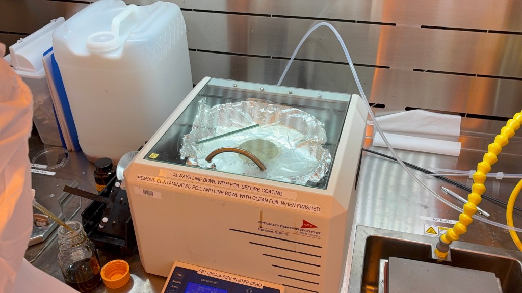
Finally, I got to work with actual fabrication equipment: Spin coater for photoresist and liftoff resist applications ; Mask aligner photolithography system; Wet bench; Load-locked titanium deposition chamber.
I also officially began my research project under Siyi Wang’s mentorship. The goal was to develop flexible nanoscale brain electrodes that could revolutionize how we: Detect brain signals; Diagnose conditions like brain cancer; Study neurological disorders. We started by spin-coating both liftoff resist and photoresist onto a wafer. We then used mask-aligner photolithography in order to get our electrode pattern on the wafer, which was developed at a wet bench in a solution. This gave us an undercut template ready for metal deposition. Later, we performed our experiment on this template, focusing on optimizing titanium film thickness for the liftoff process.


Titanium Deposition Level Experiment
We concluded our research experiment, which we began in the previous week.
- We finished learning how to use cleanroom equipment by getting official training on the load-locked evaporator
- Individually performed titanium deposition
- Performed liftoff using PG remover solution at the wet bench.
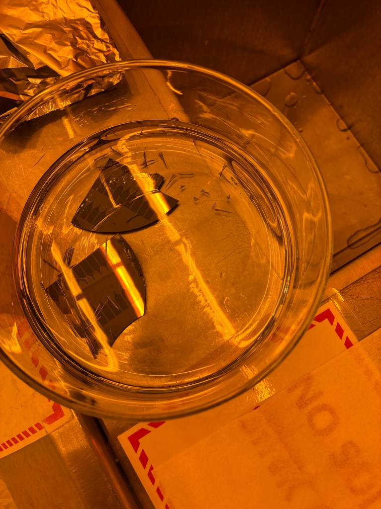
This process allowed us to complete our research experiment. Cutting the wafer from previous week into three pieces, I along with my team members Shuangyan Wang and Mathias Mansfield each performed titanium deposition on a piece with varying levels of thickness. In the current method used for the electrode fabrication, 100 nm to 300 nm thick titanium is deposited. We tested 10 nm, 20 nm, and 400 nm of titanium deposition in order to expand our range.
Experiment Analysis
We performed an analysis of our experimental results as well as characterized our materials.
- Analyzed the effectiveness of liftoff with the different thicknesses of titanium deposit and determined a more precise range for permissible titanium thickness
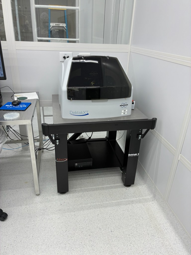
- Characterization using both an optical and stylus profilometer
- Worked on the research poster, video, and abstract
Using our results from the week before, we analyzed our outcomes with liftoff being successful at 10 nm and 20 nm; however, it was unsuccessful at 400 nm. This meant our range of thickness for successful liftoff is 10-300 nm. We determined that possible factors influencing the amount of titanium one can deposit depend on the thickness of the liftoff resist, as well as the melting and cooling effects of the resist. Further samples could create a more precise range, as well as allow for a more intensive determination of factors leading to the range.
In the next few weeks, I created my own design using AutoCAD for a maskless photolithography pattern and gold metal deposition.

Custom Maskless Photolithography Design
This week I swapped my mask aligner for a custom maskless photolithography design and focused mostly on the design and development phase.
I completed the following things:
- Prepped a wafer with sacrificial nickel, polyimide, and photoresist
- Designed my own custom pattern in AutoCAD
- Exposed my design pixel-by-pixel with UV
- Developed the resist at the wet bench, revealing my pattern
For my design, I made drawings to represent each of the fundamental forces of the universe surrounding a surprise QR code (that you should scan). The maskless photolithographer gives less resolution (being only 10 micrometers) but is much cheaper and easier to iterate on patterns due to the lack of a need to print an expensive mask.
This week was extremely fun in how creative we could be, and next week I finished off depositing gold and performing nickel etching for my final design, which concluded my time at this internship.

”Nikhil Etchent” (and a valuable cliché learned)
Final Week concluded my program…
And I failed.
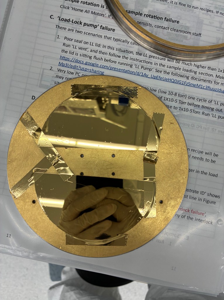
In the final steps of creating my gold maskless photolithography design I…
- Completed a gold deposition of 100nm and performed liftoff at wetbench
- Performed nickel etching to release the polyimide and gold to leave me my final design… or so I thought
Due to our rush in the final week and the nickel etching process being new to us, the nickel etchant poetically acted as a “Nikhil etchant” and because our gold was not protected with another layer of polyimide, ate away our gold, leaving me with… a crumpled-up piece of cheap polyimide rather than my gold pattern beautifully displayed on a flat piece of polyimide.
However, this ending to my internship taught me an important cliché. Engineering, and more broadly life, may be incredibly creative; however, all things require the basic fundamental skills of diligence. Most of our lives are on autopilot, so harnessing this element of human nature to perform these skills is crucial. The consequences of not doing so and being clumsy can be extremely costly (ironically, especially when time is not in your favor).
STEM Outreach: Microelectronics Education Video Series Creator
As part of STEM outreach, we were asked to create videos to introduce high school students to fabrication concepts and raise awareness of the microelectronics field. At the top of this page is the video I created to explain the “lift-off process.”
